เธขเธตเนเธซเนเธญ
 เธซเธกเธงเธเธชเธดเธเธเนเธฒ
 เธเนเธญเธกเธนเธฅ

 (Litech)-120x120.jpg)

 Full-120x120.jpg)
/01 Control Cable/02 With Shield Foil/Multi Cores/Multiconductors Foiled Shielded Single-120x120.jpg)

-120x120.jpg)


-120x120.jpg)
-120x120.jpg)
-120x120.jpg)


-120x120.jpg)
-120x120.jpg)

 เธเธฐเธเธฃเนเธฒเธชเธดเธเธเนเธฒ
 เธชเธดเธเธเนเธฒเธเธญเธเนเธฃเธฒ

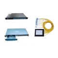
 Single Mode PLC Splitter 0101-120x120.jpg "Module-type (Cassette-type) Single Mode PLC Splitter")

/03 Building Cable/03 Coaxial Cable/05/JIS COAXIAL CABLE Satellite Broadcast Receivers Applications-120x120.jpg "JIS COAXIAL CABLE SATELLITE BROADCAST RECEIVERS APPLICATIONS 7C-FB")
")
 24 IN 010 (10 เธเธนเน)")


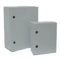
-120x120.jpg "Open System Rack LTR-OP-ALM (Aluminum)")

/01 Control Cable/01 Unshield/Multicore Conductor Unshield-120x120.jpg "เธชเธฒเธขเธกเธฑเธฅเธเธดเธเธญเธฃเน เนเธเธเนเธกเนเธกเธตเธเธดเธฅเธเน เธเธเธฒเธ 1.00 เธเธฃ.เธกเธก. (17 AWG) 2 Cores")
/01 Control Cable/03 With Shield Foil + Braid/Multi Core/Multiconductors Foiled Copper Braided Shielded-120x120.jpg "เธชเธฒเธขเนเธเนเธเธดเนเธฅ เธเธญเธเนเธเธฃเธฅ เนเธเธเธกเธตเธเธดเธฅเธเนเธเธฅเธญเธขเธเน เนเธฅเธฐ เธเธดเธฅเธเนเธเธฑเธเธเธญเธเนเธเธ 1.25 เธเธฃ.เธกเธก. (16 AWG) 6 เธเธญเธฃเน")


/02 Network Cable/04 Cable Assemblies/14 USB Cable/USB Cable-120x120.jpg "USB Cable USB Type A/B L 2 M.")

DIN Female To N Male Adaptor/L29(7;16)DIN Female To N Male Adaptor-120x120.jpg "L29(7/16)DIN Female To N Male Adaptor")

/03 Building Cable/02 Fire Alarm/01/Fire Alarm Cable-120x120.jpg "Fire Alarm Cable 1P 14 AWG")


-120x120.jpg "BLANK PANEL SIZE 4U")
/03 Building Cable/03 Coaxial Cable/09/1-120x120.jpg "CCTV / MATV CABLE C-RG59-S67")
/01 Control Cable/03 With Shield Foil + Braid/Multipairs Individual Foiled overall Foiled Copper Braided Shielded/IBI12536P-120x120.jpg "เธชเธฒเธขเนเธเนเธเธดเนเธฅ เธเธญเธเนเธเธฃเธฅ เธกเธฑเธฅเธเธดเนเธเธฃเน เนเธเธเธกเธตเธเธดเธฅเธเนเธเธฅเธญเธขเธเนเนเธเนเธฅเธฐเธเธนเน เธเธดเธฅเธเนเธเธฅเธญเธขเธเนเธฃเธงเธก เนเธฅเธฐ เธเธดเธฅเธเนเธเธฑเธเธเธญเธเนเธเธ 0.75 เธเธฃ.เธกเธก. (18 AWG) 30 เธเธนเน")


/04 Communication Cable/02 Industrial Bus Cable 150 Ohms/B228F-120x120.jpg "Industrial Bus Cable 150 Ohms B228F")
-120x120.jpg "FIX SHELVE ( OPEN RACK )")
 (Litech)-120x120.jpg "เธเธนเนเธเธฑเธเธชเธฒเธขเนเธเธฃเธจเธฑเธเธเน เธเธเธฒเธ 200 เธเธนเนเธชเธฒเธข (เนเธซเธฅเนเธ) (Litech)")
/01 Control Cable/02 With Shield Foil/Multipairs Individual Foiled Shielded/Multipairs Individual Foiled Shielded Single-120x120.jpg "เธชเธฒเธขเธกเธฑเธฅเธเธดเนเธเธฃเน เนเธเธเธกเธตเธเธดเธฅเธเนเธเธฅเธญเธขเธเนเนเธเนเธฅเธฐเธเธนเน เธเธเธฒเธ 0.50 เธเธฃ.เธกเธก. (20 AWG) 10 เธเธนเน")


-120x120.jpg "19\" HIGH QUALITY OPEN RACK 27U")


/01 Control Cable/03 With Shield Foil + Braid/Multi Pairs/Multipairs Foiled Copper Braided Shielded 01-120x120.jpg "เธชเธฒเธขเนเธเนเธเธดเนเธฅ เธเธญเธเนเธเธฃเธฅ เธกเธฑเธฅเธเธดเนเธเธฃเน เนเธเธเธกเธตเธเธดเธฅเธเนเธเธฅเธญเธขเธเน เนเธฅเธฐ เธเธดเธฅเธเนเธเธฑเธเธเธญเธเนเธเธ 0.75 เธเธฃ.เธกเธก. (18 AWG) 2 เธเธนเน")


/02 Network Cable/03 Computer Cable/02 High Speed Data Cables/Multipairs Foiled Shield (CM)-120x120.jpg "Multipairs Foiled Shield (CM) 22 AWG (7/0.254) 6 Pairs")


/22 NON-INSULATED PIN TERMINALS-38x38.jpg)


 เนเธเธฃเธฉเธเธตเธขเนเนเธเธข
 เธชเธดเธเธเนเธฒเธเนเธฒเธชเธเนเธ


-38x38.jpg)


-38x38.jpg)
 DBD Registered
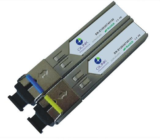
Optical Transceiver SFP 2.5Gb/s 20KM 1490nm SC
 เธเธเนเธเธทเนเธญเธเธขเธฒเธขเธเธเธฒเธ |
|
Product Specification Sheet
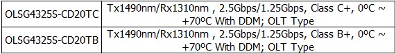
OLSG4325S-CD20TC
RoHS Compliant GPON SFP OLT C+ Optical Transceiver
PRODUCT FEATURES
๏ต Single Fiber Transceiver with single mode SC receptacle
๏ต 1490nm continuous-mode transmitter with DFB laser
๏ต 1310nm burst-mode receiver with APD-TIA
๏ต Single 3.3V power supply
๏ต Reset burst-mode receiver design
๏ต Burst mode signal detect output which is LVTTL compatible.
๏ต Burst mode received signal strength indication (RSSI) output
๏ต 20Km Reach 28dB link budget
๏ต Complies with ITU-T G984.2 Class C+
๏ต Digital diagnostic interface compliant with SFF-8472 Rev 9.4 ,
๏ต Complies with RoHS directive (2002/95/EC)
๏ต Operating case temperature: Standard : 0 to +70°C
APPLICATIONS
๏ต Gigabit Passive Optical Networks (G-PON) - OLT side
PRODUCT DESCRIPTIONS
The OLSG4325S-CD20TC transceiver is the high performance module for single fiber by using 1490nm continuous-mode transmitter and 1310nm burst-mode receiver. It is optical line terminal(OLT) for ITU-T G984.2. The optical transceiver is compliant with the Small Form- Factor Pluggable (SFP) Multi-Source Agreement (MSA).
The transmitter section uses a 1490nm DFB LD with automatic power control (APC) function and temperature compensation circuitry to ensure stable extinction ratio over all operating temperature range. and is Classโ laser compliant IEC825 and CDRH standards. The receiver has a hermetically packaged burst-mode APD-TIA (trans-impedance amplifier) pre-amplifier and a burst-mode limiting amplifier with LVPECL compatible differential outputs.
The receiver also includes the function of burst mode signal detect output and fast RSSI output which is enabled by a trigger. When the burst optical power is on, the receiver outputs high level; when the burst optical power is off, the receiver outputs low level. Fast RSSI function can satisfy more severe timing demand to monitor the power from any ONU.
ABSOLUTE MAXIMUM RATINGS
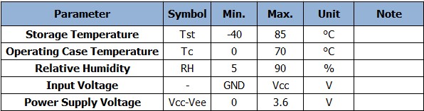
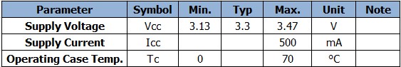
RECOMMENDED OPERATING CONDITIONS
ELECTRICAL INPUT/OUTPUT CHARACTERISTICS
๏ฌ Transmitter
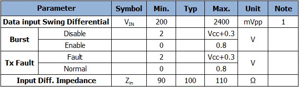
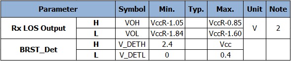
๏ฌ Receiver
Note 1) PECL input, internally AC-coupled and terminated
Note 2) Internally DC-coupled.
OPTICAL CHARACTERISTICS
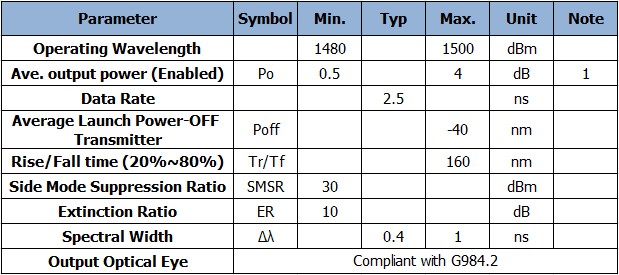
๏ฌ Transmitter
๏ฌ Receiver
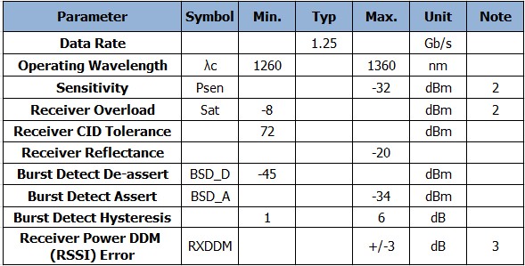
Note 1) The optical power is launched into SMF .
Note 2) Measured with a PRBS 223-1 test pattern @1250Mbps, BER ≤1×10⁻¹⁰.
Note 3) RSSI DDM working range is between -8 to -28 dBm. RSSI DDM accuracy is better than +/- 3dB for input power levels between -12 to -28 dBm, the accuracy reduces to +/- 5 dBm for other input power levels.
DIAGNOSTIC SPECIFICATION
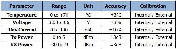
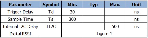
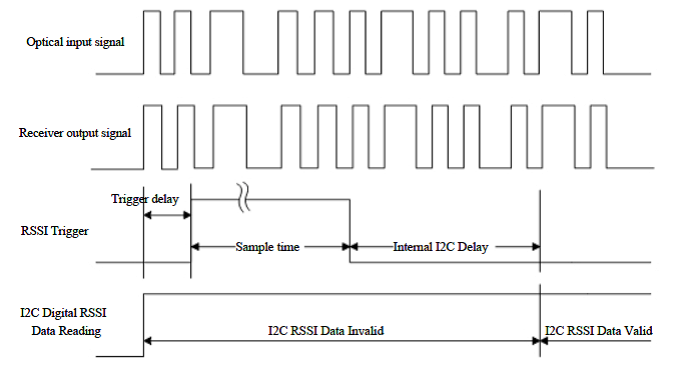
Figure 1. Digital RSSI Timing
TIMING CHARACTERISTICS FOR RESET
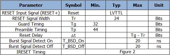
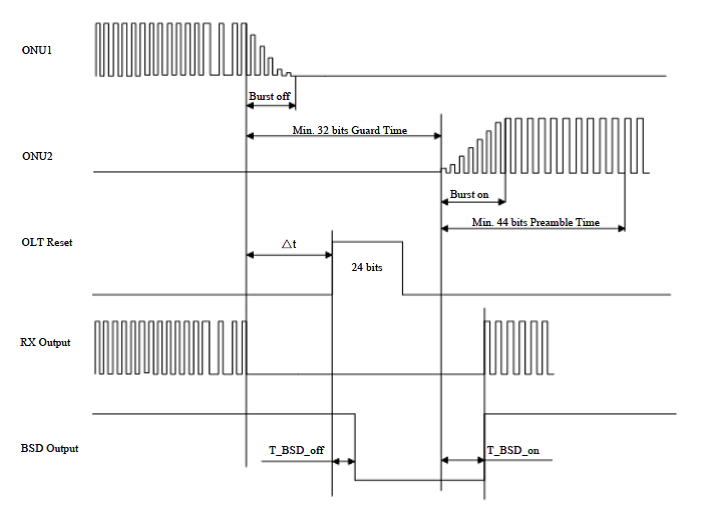
Figure 2 Reset Timing
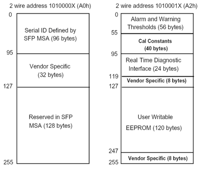
DIGITAL DIAGNOSTIC MEMORY MAP
The transceivers provide serial ID memory contents and diagnostic information about the present operating conditions by the 2-wire serial interface (SCL, SDA).
The diagnostic information with internal calibration or external calibration all are implemented, including received power monitoring, transmitted power monitoring, bias current monitoring, supply voltage monitoring and temperature monitoring.
The digital diagnostic memory map specific data field defines as following.
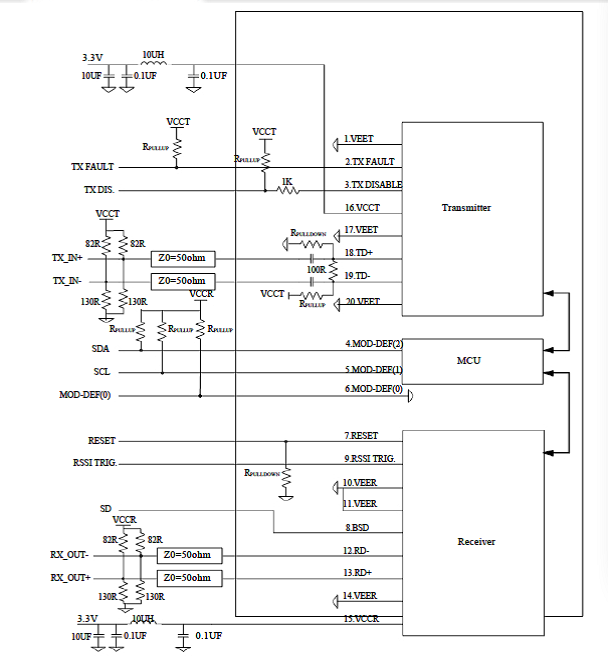
PIN DIAGRAM
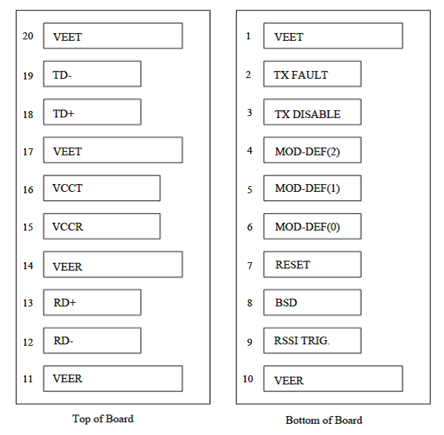
PIN DESCRIPTIONS
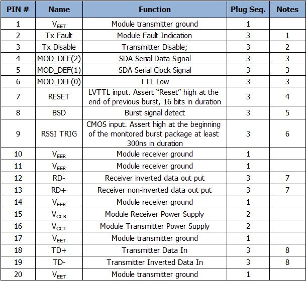
Plug Seq.: Pin engagement sequence during hot plugging.
1) TX Fault is an open collector output, which should be pulled up with a 4.7k~10kΩ resistor on the host board to a voltage between 2.0V and Vcc+0.3V. Logic 0 indicates normal operation; Logic 1 indicates a laser fault of some kind. In the low state, the output will be pulled to less than 0.8V.
2) TX Disable is an input that is used to shut down the transmitter optical output. It is pulled up within the module with a 4.7k~10kΩ resistor. Its states are:
Low (0 to 0.8V): Transmitter on
(>0.8V, < 2.0V): Undefined
High (2.0 to 3.465V): Transmitter Disabled
Open: Transmitter Disabled
3) Mod-Def 0,1,2. These are the module definition pins. They should be pulled up with a 4.7k~10kΩ resistor on the host board. The pull-up voltage shall be VccT or VccR.
Mod-Def 0 is grounded by the module to indicate that the module is present Mod-Def 1 is the clock line of two wire serial interface for serial ID
Mod-Def 2 is the data line of two wire serial interface for serial ID
4) RESET is a LVTTL input. When the previous burst signal package is end, the host will give a “high” RESET to restore the state of LA. Internal pull-down 10K resistor to GND.
5) BSD can track the state of receiving burst signal. Logic 0 indicates loss of signal; Logic1 indicates receiving signal packages.
6) RSSI TRIG is a CMOS input. Assert high after 30ns delay time of the beginning of the monitored burst package at least 300ns in duration.
7) RD-/+: These are the differential receiver outputs. They are internally DC-coupled 100 differential lines which should be terminated with 100Ω (differential) at the user SERDES.
8) TD-/+: These are the differential transmitter inputs. They are internally AC-coupled, differential lines with 100Ω differential termination inside the module.
RECOMMENDED INTERFACE CIRCUIT
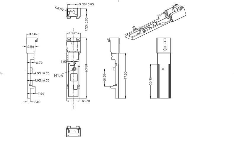
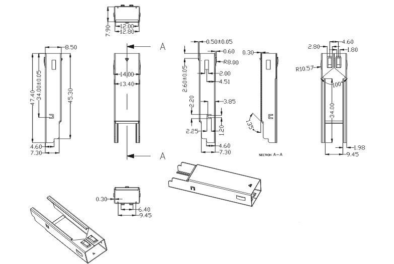
PACKAGE DIMENSIONS
ORDERING INFORMATION
เธเธงเธฒเธกเธเธดเธเนเธซเนเธ: เธเธณเนเธเธฐเธเธณ: HTML เธเธฐเนเธกเนเธเธนเธเนเธเธฅเธ!
เธเธงเธฒเธกเธเธดเธขเธก: เนเธขเน เธเธต
เธเนเธญเธเธฃเธซเธฑเธชเนเธเธเธฅเนเธญเธเธเนเธฒเธเธฅเนเธฒเธเธเธตเน: