เธขเธตเนเธซเนเธญ
 เธซเธกเธงเธเธชเธดเธเธเนเธฒ
 เธเนเธญเธกเธนเธฅ

 (Litech)-120x120.jpg)

 Full-120x120.jpg)
/01 Control Cable/02 With Shield Foil/Multi Cores/Multiconductors Foiled Shielded Single-120x120.jpg)

-120x120.jpg)

-120x120.jpg)
-120x120.jpg)
-120x120.jpg)


-120x120.jpg)
-120x120.jpg)


 เธเธฐเธเธฃเนเธฒเธชเธดเธเธเนเธฒ
 เธชเธดเธเธเนเธฒเธเธญเธเนเธฃเธฒ
/01 Control Cable/03 With Shield Foil + Braid/Multipairs Individual Foiled overall Foiled Copper Braided Shielded/IBI12536P-120x120.jpg "เธชเธฒเธขเนเธเนเธเธดเนเธฅ เธเธญเธเนเธเธฃเธฅ เธกเธฑเธฅเธเธดเนเธเธฃเน เนเธเธเธกเธตเธเธดเธฅเธเนเธเธฅเธญเธขเธเนเนเธเนเธฅเธฐเธเธนเน เธเธดเธฅเธเนเธเธฅเธญเธขเธเนเธฃเธงเธก เนเธฅเธฐ เธเธดเธฅเธเนเธเธฑเธเธเธญเธเนเธเธ 0.75 เธเธฃ.เธกเธก. (18 AWG) 16 เธเธนเน")
/05 Special Cable/06 UL 1015 CSA TEW/UL 1015 CSA TEW-120x120.jpg "Appliance Wiring Material UL 1015 CSA TEW Solid 5.16 sq.mm. (10 AWG)")
")
/03 Building Cable/02 Fire Alarm/02/Fire Alarm Cable-D-120x120.jpg "Fire Alarm Cable 1P 16 AWG-D")


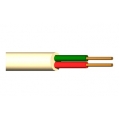
/03 Building Cable/01 Building and Audio/02/0-120x120.jpg "MICROPHONE CABLE 1P 22 AWG")

")

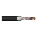
/01 Control Cable/03 With Shield Foil + Braid/Multi Core/Multiconductors Foiled Copper Braided Shielded-120x120.jpg "เธชเธฒเธขเนเธเนเธเธดเนเธฅ เธเธญเธเนเธเธฃเธฅ เนเธเธเธกเธตเธเธดเธฅเธเนเธเธฅเธญเธขเธเน เนเธฅเธฐ เธเธดเธฅเธเนเธเธฑเธเธเธญเธเนเธเธ 0.50 เธเธฃ.เธกเธก. (20 AWG) 9 เธเธญเธฃเน")
/03 Building Cable/03 Coaxial Cable/07/JIS COAXIAL CABLE Radio Applications-120x120.jpg "JIS COAXIAL CABLE RADIO APPLICATIONS 3D-FB")


/02 Network Cable/03 Computer Cable/02 High Speed Data Cables/Multipairs Foiled Shield (CM)-120x120.jpg "Multipairs Foiled Shield (CM) 24 AWG (7/0.2) 8 Pairs")


/05 Special Cable/03 Self Support Crane Control Cable/Self Support Crane Control Cable 02-120x120.jpg "Self Support Crane Control Cable PVC Insulated, PVC Jacket 600V-Double Sling 1.50 sq.mm. 5 Cores")
")
-120x120.jpg "MMCX Female PCB Mount (Type B)")
/05 Special Cable/04 Multiconductors with Steel Wire Braided Double Sheath/Multiconductors with Steel wire Braided Double sheath 02-120x120.jpg "Multiconductors with Steel Wire Braided Double Sheath 0.50 sq.mm. (20 AWG) 30 Cores")


/01 Control Cable/01 Unshield/Multicore Conductor Unshield-120x120.jpg "เธชเธฒเธขเธกเธฑเธฅเธเธดเธเธญเธฃเน เนเธเธเนเธกเนเธกเธตเธเธดเธฅเธเน เธเธเธฒเธ 0.5 เธเธฃ.เธกเธก. (20 AWG) 9 Cores")


/05 Coaxial to Fiber Converter-120x120.jpg "Coaxial to Fiber Converter")


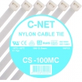
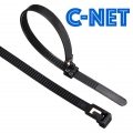
 เธชเธตเธเธฒเธง HYK100 (C-NET Cable Tie)")

-120x120.jpg "Free Standing FSF DDF Frame 256 E1")


/08 VINYL-INSULATED BLADE TERMINALS-38x38.jpg)


/22 NON-INSULATED PIN TERMINALS-38x38.jpg)
 เนเธเธฃเธฉเธเธตเธขเนเนเธเธข
 เธชเธดเธเธเนเธฒเธเนเธฒเธชเธเนเธ


-38x38.jpg)


-38x38.jpg)
 DBD Registered
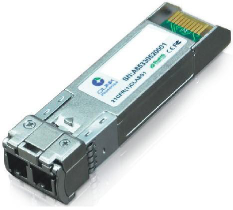
Optical Transceiver SFP+ 10.3125Gb/s 40KM 1550nm LC
 เธเธเนเธเธทเนเธญเธเธขเธฒเธขเธเธเธฒเธ |
|
Product Specification Sheet
OLSCxx1XL-CD40
RoHS Compliant 10Gb/s SFP+ CWDM 40KM Optical Transceiver
PRODUCT FEATURES
โ Hot pluggable
โ 10Gb/s serial optical interface
โ Up to 40km on 9/125um SMF
โ Compliant with SFP+ MSA
โ SFP MSA package with duplex LC connector
โ Digital Diagnostic Monitor Interface
โ Very low EMI and excellent ESD protection
โ High transmission margin
โ +3.3V single power supply
โ Below <1.5W power consumption
โ SFP mechanical interface
โ Wide data-rate range
APPLICATIONS
โ 10G Base-ER/EW
โ 10G Fiber Channel
โ Other optical links
STANDARD
โ SFP+ MSA Compliant
โ SFF-8472 reversion 9.5 compliant
โ IEEE802.3-2005 compliant
โ Telcordia GR-468-CORE compliant
โ FCC 47 CFR Part 15,Class B compliant
โ FDA 21 CFR 1040.10 and 1040.11,class1 compliant
โ RoHS compliant
PRODUCT DESCRIPTIONS
โ OlinkPhotonics OLSCxx1XL-CD40 optical transceivers are designed for 10Gb/s serial optical interfaces for data communications with single mode fiber (SMF). The trans-ceiver can support 1.25Gb/s to 11.1Gb/s.
โ The transceiver designs are optimized for high performance and cost effective to supply customers the best solutions for datacom and storage applications.
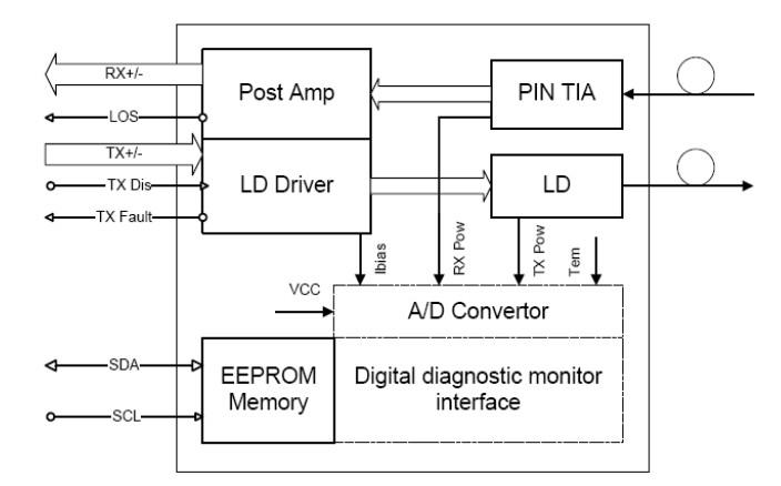
FUNCTIONAL DIAGRAM
ABSOLUTE MAXIMUM RATINGS
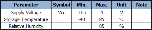
Note: Stress in excess of the maximum absolute ratings can cause permanent damage to the module
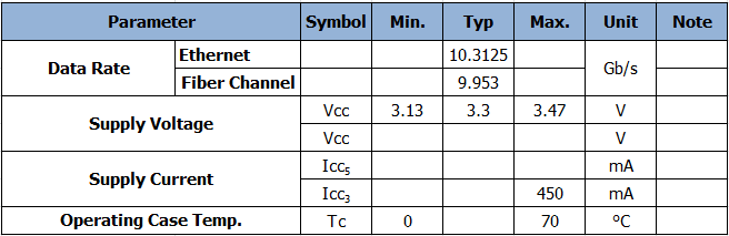
GERERAL OPERATING CHARACTERISTICS
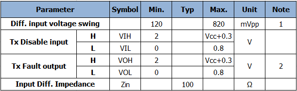
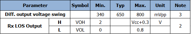
ELECTRICAL INPUT/OUTPUT CHARACTERISTICS
๏ฌ Transmitter
๏ฌ Receiver
Note 1) TD+/- are internally AC coupled with 100Ω differential termination inside the module.
Note 2) Tx Fault and Rx LOS are open collector outputs, which should be pulled up with 4.7k to 10kΩ resistors on the host board. Pull up voltage between 2.0V and Vcc+0.3V.
Note 3) RD+/- outputs are internally AC coupled, and should be terminated with 100Ω (differential) at the user SERDES.
OPTICAL CHARACTERISTICS
๏ฌ Transmitter
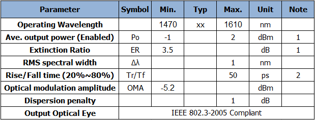
๏ฌ Receiver
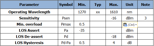
Note 1) Class 1 Laser Safety per FDA/CDRH and IEC-825-1 regulations.
Note 2) 20%~80%
Note 3) Measured with a PRBS 231-1 test pattern, @6.25Gb/s, BER<10-12
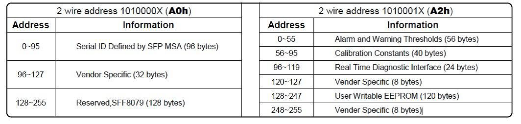
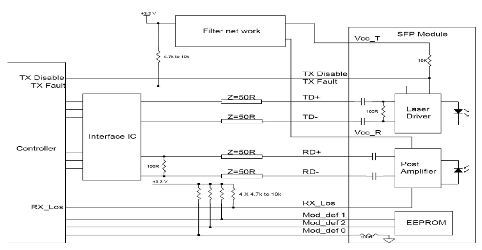
SFP Module Control and Management
The SFP modules implement the 2-wire serial communication protocol as defined in the SFP
MSA.
The serial ID information of the SFP modules and Digital Diagnostic Monitor parameters can be
accessed through the I2C interface at address A0h and A2h. The memory is mapped in Table 1.
Detailed ID information(A0h) is listed in Ta-ble 2. And the DDM specification(A2h) is described
in Table 3. For more details of the memory map and byte definitions, please refer to the
SFF-8472 (Rev 9.3, Aug. 2002), “Digital Diagnostic Monitoring Interface for Optical
Transceivers”.
The DDM parameters have been internally calibrated.
Table 1. Digital Diagnostic Memory Map (Specific Data Field Descriptions)
PIN DEFINITIONS AND FUNCTIONS
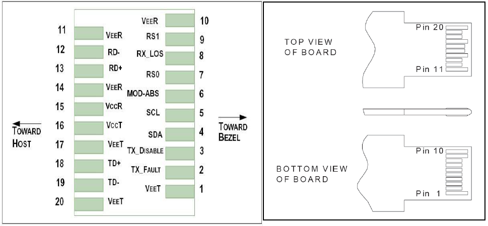
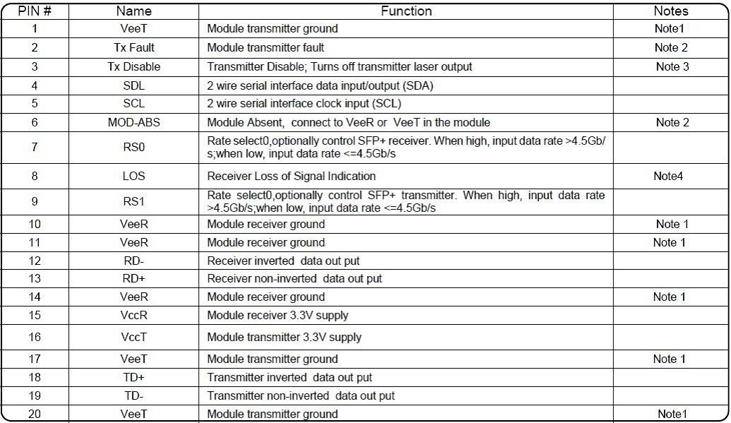
Note 1) The module ground pins shall be isolated from the module case.
Note 2) This pin is an open collector/drain output pin and shall be pulled up with
4.7K-10Kohms to Host_Vcc on the host board.
Note 3) This pin shall be pulled up with 4.7K-10Kohms to VccT in the module.
Note 4) This pin is an open collector/drain output pin and shall be pulled up with
4.7K-10Kohms to Host_Vcc on the host board. In FC designated as RX_LOS, inSONET
designated as LOS, and in Ethernet designated at Signal Detect.
TYPICAL INTERFACE CIRCUIT
Recommended power supply filter
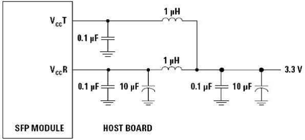
Note: Inductors with DC resistance of less than 1Ω should be used in order to maintain the
required voltage at the SFP input pin with 3.3V supply voltage. When the recommended
supply filtering network is used, hot plugging of the SFP transceiver module will result in an
inrush current of no more than 30 mA greater than the steady state value
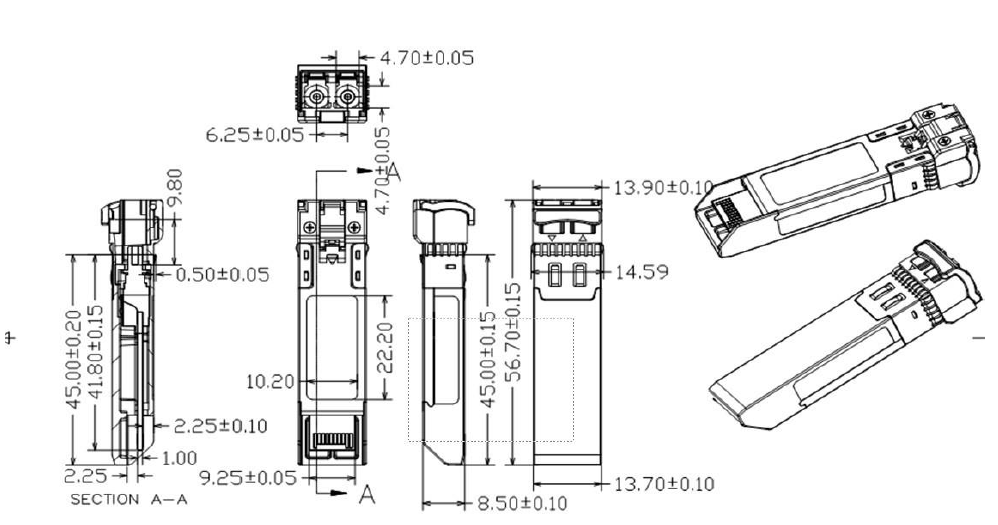
PACKAGE DIMENSION
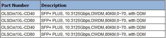
ORDERING INFORMATION
เธเธงเธฒเธกเธเธดเธเนเธซเนเธ: เธเธณเนเธเธฐเธเธณ: HTML เธเธฐเนเธกเนเธเธนเธเนเธเธฅเธ!
เธเธงเธฒเธกเธเธดเธขเธก: เนเธขเน เธเธต
เธเนเธญเธเธฃเธซเธฑเธชเนเธเธเธฅเนเธญเธเธเนเธฒเธเธฅเนเธฒเธเธเธตเน: