เธขเธตเนเธซเนเธญ
 เธซเธกเธงเธเธชเธดเธเธเนเธฒ
 เธเนเธญเธกเธนเธฅ

 (Litech)-120x120.jpg)

 Full-120x120.jpg)
/01 Control Cable/02 With Shield Foil/Multi Cores/Multiconductors Foiled Shielded Single-120x120.jpg)

-120x120.jpg)


-120x120.jpg)
-120x120.jpg)
-120x120.jpg)


-120x120.jpg)
-120x120.jpg)

 เธเธฐเธเธฃเนเธฒเธชเธดเธเธเนเธฒ
 เธชเธดเธเธเนเธฒเธเธญเธเนเธฃเธฒ
-120x120.jpg "19\" Coaxial Panel 16 Port BNC (Fixed)")
/11 SUN-HFBR4506-120x120.jpg "SUN-HFBR4501&SUN-HFBR4511")


/01 Control Cable/01 Unshield/Multicore Conductor Unshield-120x120.jpg "เธชเธฒเธขเธกเธฑเธฅเธเธดเธเธญเธฃเน เนเธเธเนเธกเนเธกเธตเธเธดเธฅเธเน เธเธเธฒเธ 1.00 เธเธฃ.เธกเธก. (17 AWG) 4 Cores")

-120x120.jpg "D-Type Indoor Cable (2 ~ 12 Cores)")
/FTTH Cable/Indoor Soft Cable/07 FTTX Cable Bow-Type Drop Cable-120x120.jpg "FTTX Cable Bow-Type Drop Cable")
 INDUSTRIAL CO., LTD (Video Balun)/01 Video Balun/15 Passive Transceiver TT223-120x120.jpg "Passive Transceiver TT223")


 22 IN 006 (6 เธเธนเน)")
/01 Control Cable/02 With Shield Foil/Multipairs Individual Foiled Shielded/Multipairs Individual Foiled Shielded Single-120x120.jpg "เธชเธฒเธขเธกเธฑเธฅเธเธดเนเธเธฃเน เนเธเธเธกเธตเธเธดเธฅเธเนเธเธฅเธญเธขเธเนเนเธเนเธฅเธฐเธเธนเน เธเธเธฒเธ 0.50 เธเธฃ.เธกเธก. (20 AWG) 10 เธเธนเน")


/05 Special Cable/06 UL 1015 CSA TEW/UL 1015 CSA TEW-120x120.jpg "Appliance Wiring Material UL 1015 CSA TEW Solid 5.16 sq.mm. (10 AWG)")
/Fiber Optic Patch Panel(Slidable type) 00-120x120.jpg "Fiber Optic Patch Panel(Slidable type)")


/01 Control Cable/02 With Shield Foil/Multi Pairs/Multipairs Foiled Shielded Single-120x120.jpg "เธชเธฒเธขเธกเธฑเธฅเธเธดเนเธเธฃเน เนเธเธเธกเธตเธเธดเธฅเธเนเธเธฅเธญเธขเธเน เธเธเธฒเธ 0.75 เธเธฃ.เธกเธก. (18 AWG) 8 เธเธนเน")


")


/03 Building Cable/04 Security-Alarm Cables/General purpose low voltage circuit wiring-120x120.jpg "General purpose low voltage circuit wiring 24 AWG, 2C , 7/0.20mm , DCR 87.6 ohm/km")


/01 Control Cable/03 With Shield Foil + Braid/Multi Pairs/Multipairs Foiled Copper Braided Shielded 01-120x120.jpg "เธชเธฒเธขเนเธเนเธเธดเนเธฅ เธเธญเธเนเธเธฃเธฅ เธกเธฑเธฅเธเธดเนเธเธฃเน เนเธเธเธกเธตเธเธดเธฅเธเนเธเธฅเธญเธขเธเน เนเธฅเธฐ เธเธดเธฅเธเนเธเธฑเธเธเธญเธเนเธเธ 0.50 เธเธฃ.เธกเธก. (20 AWG) 24 เธเธนเน")


/08 VINYL-INSULATED BLADE TERMINALS-38x38.jpg)


/22 NON-INSULATED PIN TERMINALS-38x38.jpg)
 เนเธเธฃเธฉเธเธตเธขเนเนเธเธข
 เธชเธดเธเธเนเธฒเธเนเธฒเธชเธเนเธ


-38x38.jpg)


-38x38.jpg)
 DBD Registered
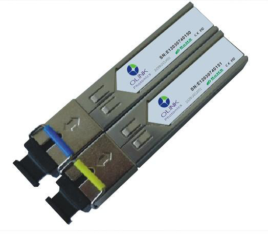
Optical Transceiver SFP 155M 20KM 1310&1550 SC
 เธเธเนเธเธทเนเธญเธเธขเธฒเธขเธเธเธฒเธ |
|
Product Specification Sheet
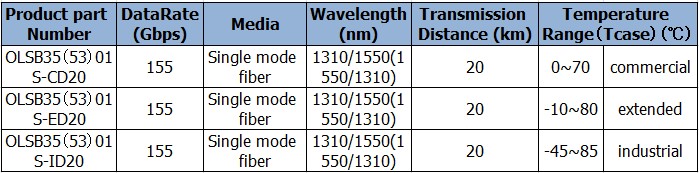
OLSB35(53)01S-CD20
RoHS Compliant 155M 1310/1550nm(1550/1310nm) 20KM Transceiver
PRODUCT FEATURES
โUp to 155Mb/s data links
โFP laser transmitter
โPIN photo-detector
โUp to 20km on 9/125μm SMF
โHot-pluggable SFP footprint
โBIDI SC/UPC type pluggable optical interface
โLow power dissipation
โMetal enclosure, for lower EMI
โRoHS compliant and lead-free
โSingle +3.3V power supply
โSupport Digital Diagnostic Monitoring interface
โCompliant with SFF-8472
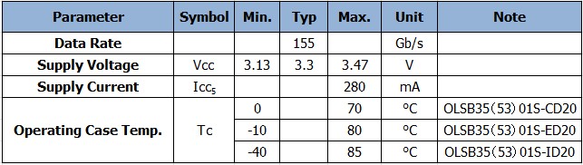
โCase operating temperature
Commercial: 0°C to +70°C
Extended: -10°C to +80°C
Industrial: -40°C to +85°C
APPLICATIONS
โSwitch to Switch Interface
โFast Ethernet
โSwitched Backplane Applications
โRouter/Server Interface
โOther Optical Links
STANDARD
โ SFP+ MSA Compliant
โ SFF-8472 reversion 9.5 compliant
โ IEEE802.3-2005 compliant
โ Telcordia GR-468-CORE compliant
โ FCC 47 CFR Part 15,Class B compliant
โ FDA 21 CFR 1040.10 and 1040.11,class1 compliant
โ RoHS compliant
PRODUCT DESCRIPTIONS
โ Olink Photonics’s OLSB35๏ผ53๏ผ01S-CD20 optical transceivers are designed for optical interfaces for data communications with
โ single mode fiber (SMF). The transceiver designs are optimized for high performance and cost effective to supply customers the best solutions for telecom applications.
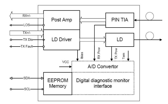
FUNCTIONAL DIAGRAM
Ordering information
ABSOLUTE MAXIMUM RATINGS
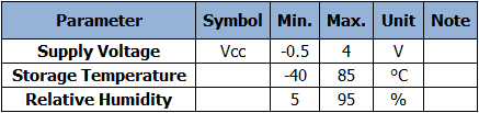
Note: Stress in excess of the maximum absolute ratings can cause permanent damage to the module
GERERAL OPERATING CHARACTERISTICS
ELECTRICAL INPUT/OUTPUT CHARACTERISTICS
๏ฌ Transmitter
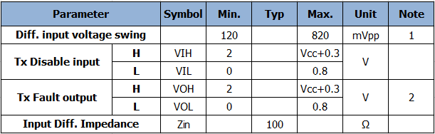
๏ฌ Receiver
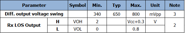
Note 1) TD+/- are internally AC coupled with 100Ω differential termination inside the module.
Note 2) Tx Fault and Rx LOS are open collector outputs, which should be pulled up with 4.7k to 10kΩ resistors on the host board. Pull up voltage between 2.0V and Vcc+0.3V.
Note 3) RD+/- outputs are internally AC coupled, and should be terminated with 100Ω (differential) at the user SERDES.
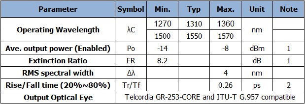
OPTICAL CHARACTERISTICS
๏ฌ Transmitter
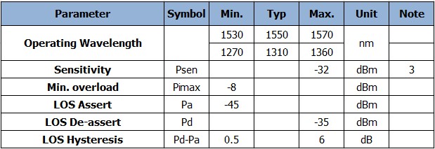
Note (1): Measure at 2^23-1 NRZ PRBS pattern
Note (2): Transmitter eye mask definition
๏ฌ Receiver
Note 1) Measured at 10.3125b/s with PRBS 231 – 1 NRZ test pattern.
Note 2) 20%~80%
Note 3) Under the ER worst case, measured at 10.3125 Gb/s with PRBS 231 - 1 NRZ test pattern for BER < 1x10-12
Digital Diagnostic Functions
OLINK’S OLSB35(53)01S-CD20 transceivers support the 2-wire serial communication protocol as defined in the SFP MSA. It is very closely related to the E2PROM defined in the GBIC standard, with the same electrical specifications.
The standard SFP serial ID provides access to identification information that describes the transceiver’s capabilities, standard interfaces, manufacturer, and other information.
Additionally, OLINKPHOTONICS SFP transceivers provide a unique enhanced digital diagnostic
monitoring interface, which allows real-time access to device operating parameters such as
transceiver temperature, laser bias current, transmitted optical power, received optical power
and transceiver supply voltage. It also defines a sophisticated system of alarm and warning flags,
which alerts end-users when particular operating parameters are outside of a factory set
normal range.
The SFP MSA defines a 256-byte memory map in E2PROM that is accessible over a 2-wire serial
interface at the 8bit address 1010000X (A0h). The digital diagnostic monitoring interface makes
use of the 8 bit address 1010001X (A2h), so the originally defined serial ID memory map
remains unchanged. The interface is identical to, and is thus fully backward compatible with
both the GBIC Specification and the SFP Multi Source Agreement.
The operating and diagnostics information is monitored and reported by a Digital Diagnostics
Transceiver Controller (DDTC) inside the transceiver, which is accessed through a 2-wire serial
interface. When the serial protocol is activated, the serial clock signal (SCL, Mod Def 1) is
generated by the host. The positive edge clocks data into the SFP transceiver into those
segments of the E2PROM that are not write-protected. The negative edge clocks data from the
SFP transceiver. The serial data signal (SDA, Mod Def 2) is bi-directional for serial data transfer.
The host uses SDA in conjunction with SCL to mark the start and end of serial protocol
activation. The memories are organized as a series of 8-bit data words that can be addressed
individually or sequentially.
Digital diagnostics for the OLSB35(53)01S-CD20 are Internally calibrated by default.
Pin Definitions and Functions
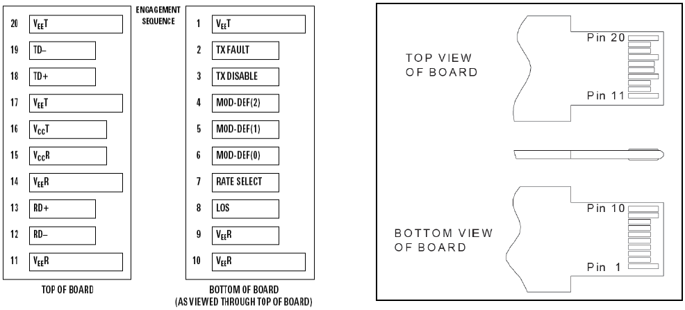
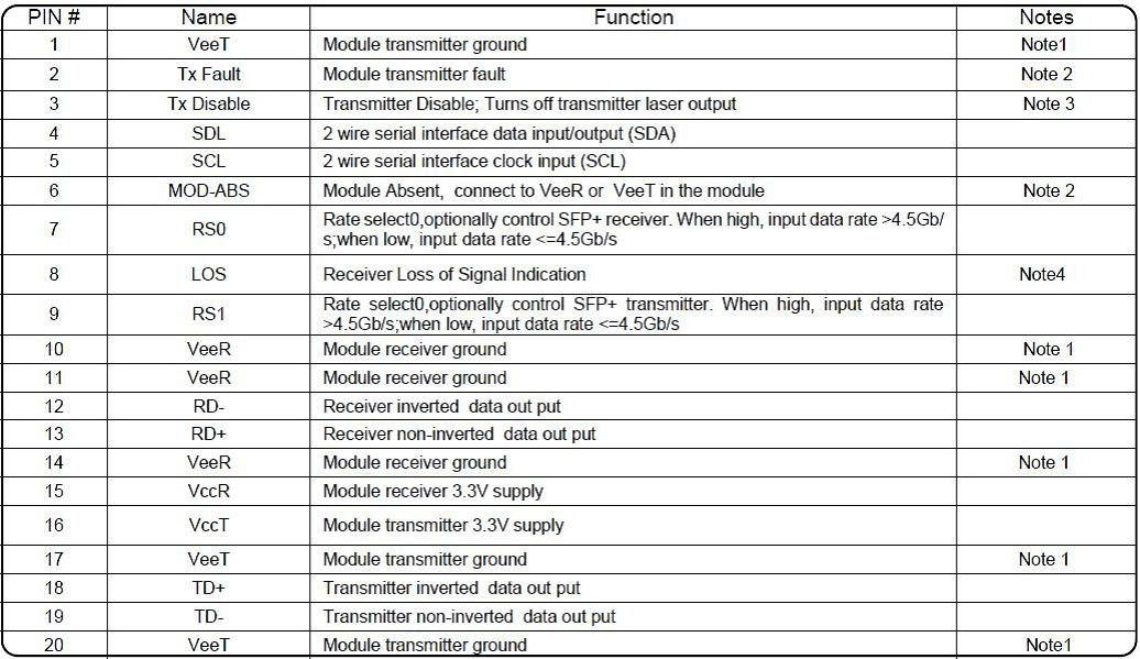
OL INK PHOTONICS Rev 1. 0 Jan 1, 2013
Note 1) The module ground pins shall be isolated from the module case.
Note 2) This pin is an open collector/drain output pin and shall be pulled up with
4.7K-10Kohms to Host_Vcc on the host board.
Note 3) This pin shall be pulled up with 4.7K-10Kohms to VccT in the module.
Note 4) This pin is an open collector/drain output pin and shall be pulled up with
4.7K-10Kohms to Host_Vcc on the host board. In FC designated as RX_LOS, inSONET
designated as LOS, and in Ethernet designated at Signal Detect.
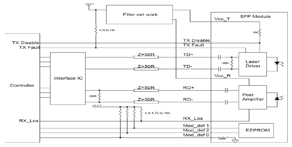
TYPICAL INTERFACE CIRCUIT
Recommended power supply filter
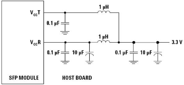
Note: Inductors with DC resistance of less than 1Ω should be used in order to maintain the required voltage at the SFP input pin with 3.3V supply voltage. When the recommended supply filtering network is used, hot plugging of the SFP transceiver module will result in an inrush current of no more than 30 mA greater than the steady state value
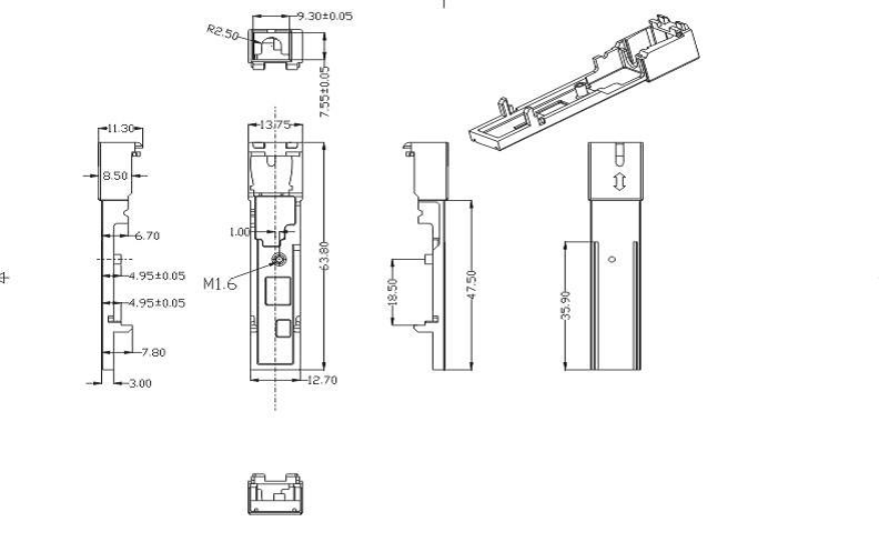
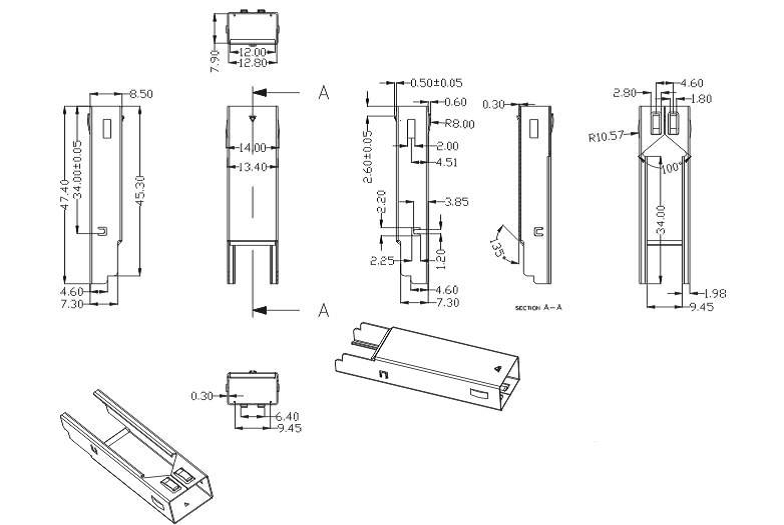
PACKAGE DIMENSIONS
เธเธงเธฒเธกเธเธดเธเนเธซเนเธ: เธเธณเนเธเธฐเธเธณ: HTML เธเธฐเนเธกเนเธเธนเธเนเธเธฅเธ!
เธเธงเธฒเธกเธเธดเธขเธก: เนเธขเน เธเธต
เธเนเธญเธเธฃเธซเธฑเธชเนเธเธเธฅเนเธญเธเธเนเธฒเธเธฅเนเธฒเธเธเธตเน: